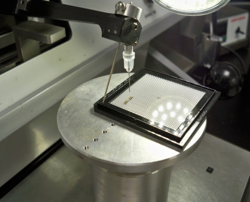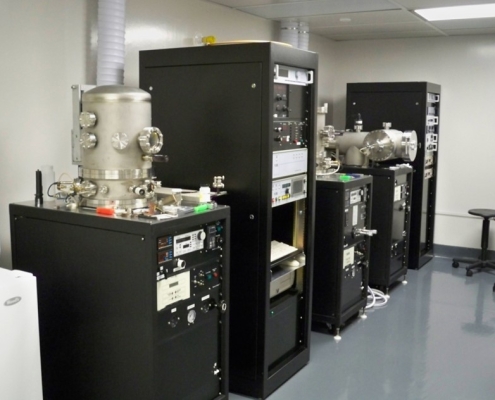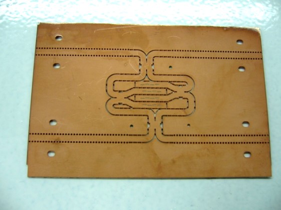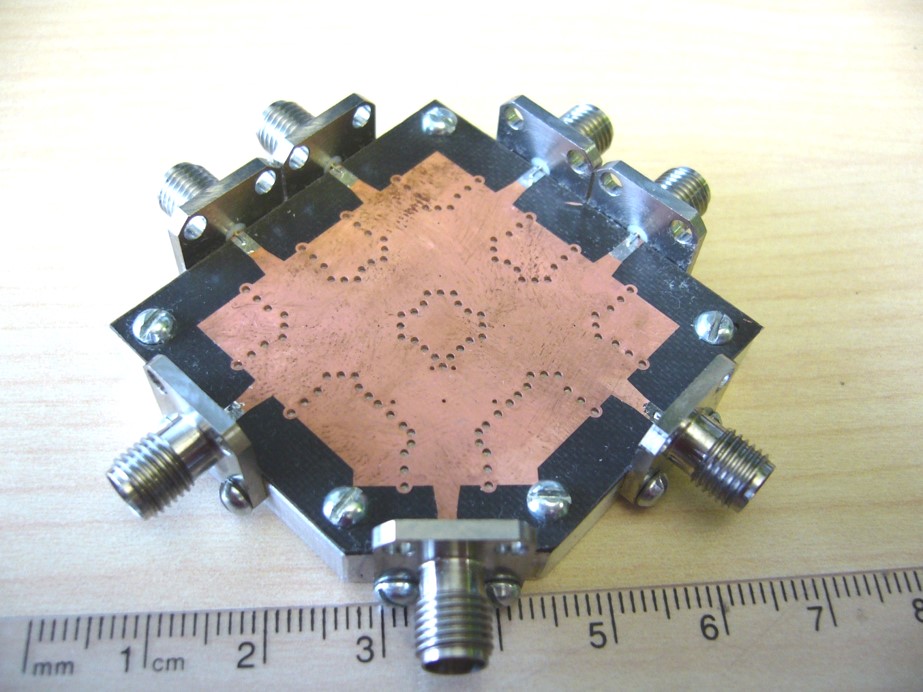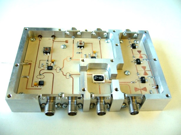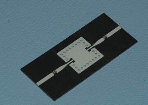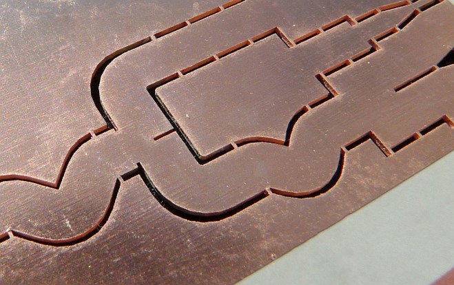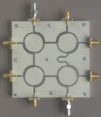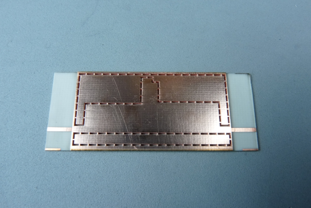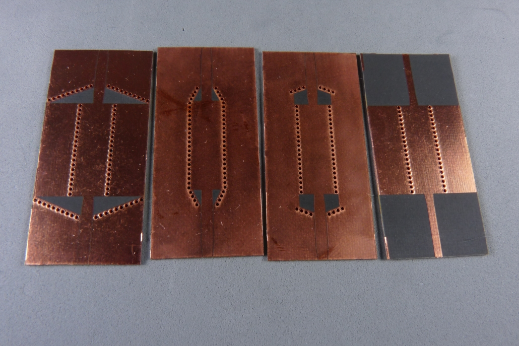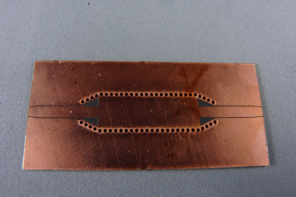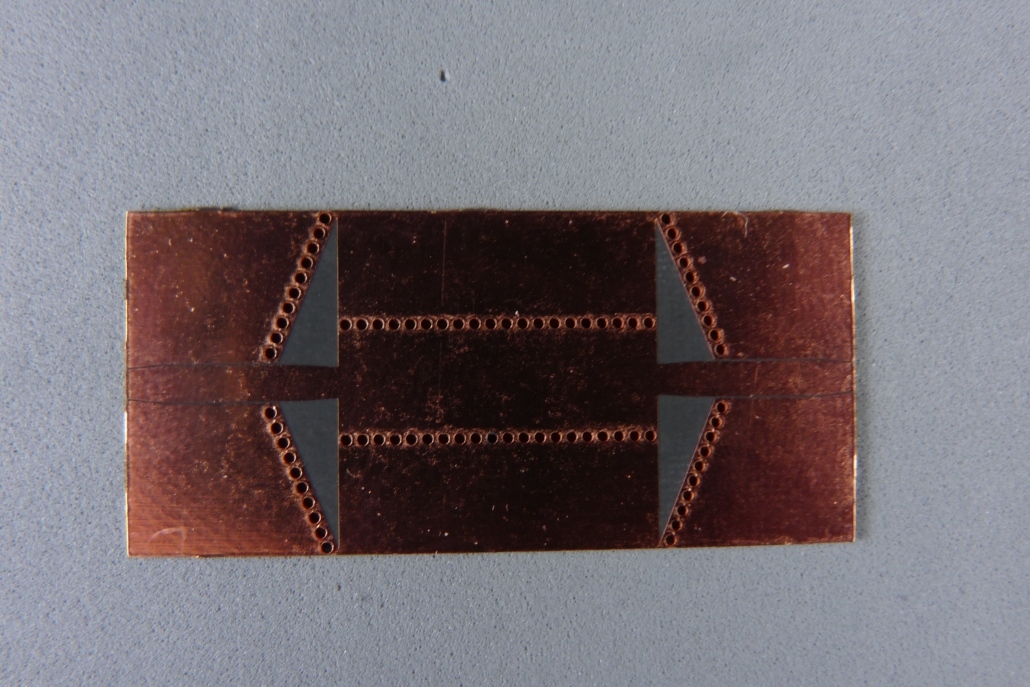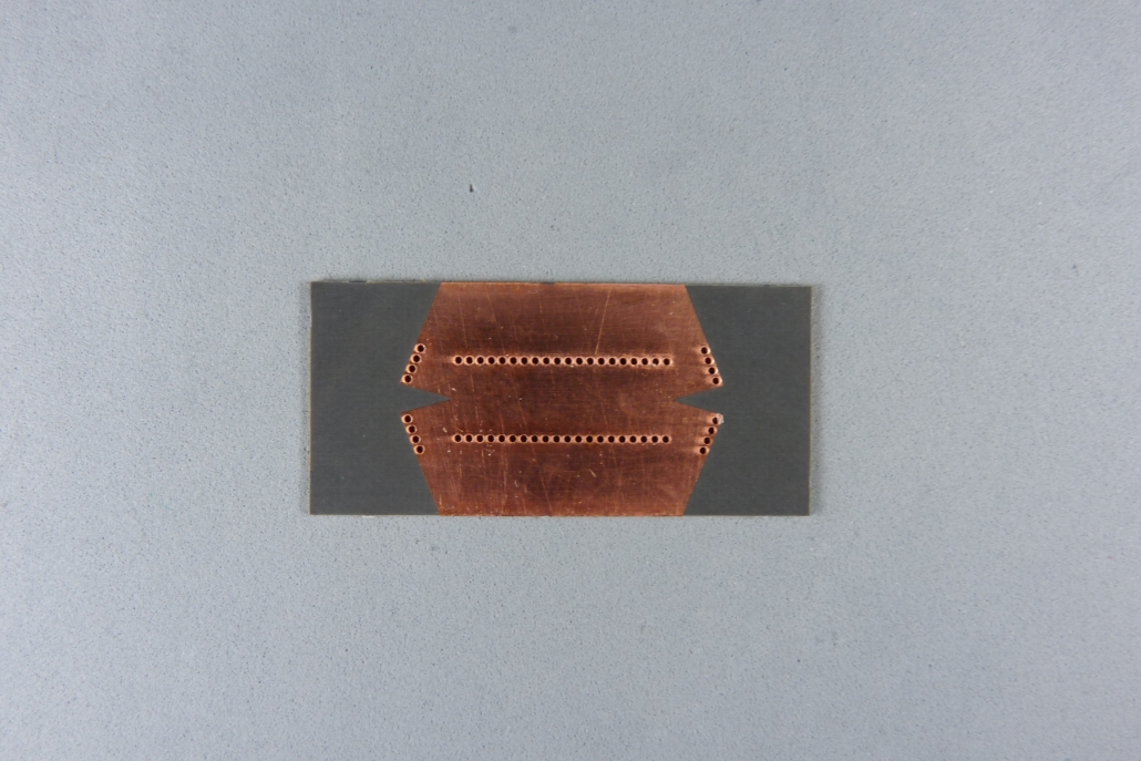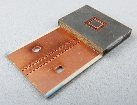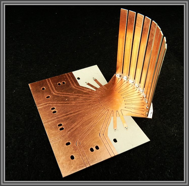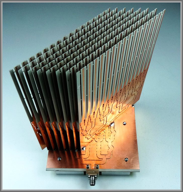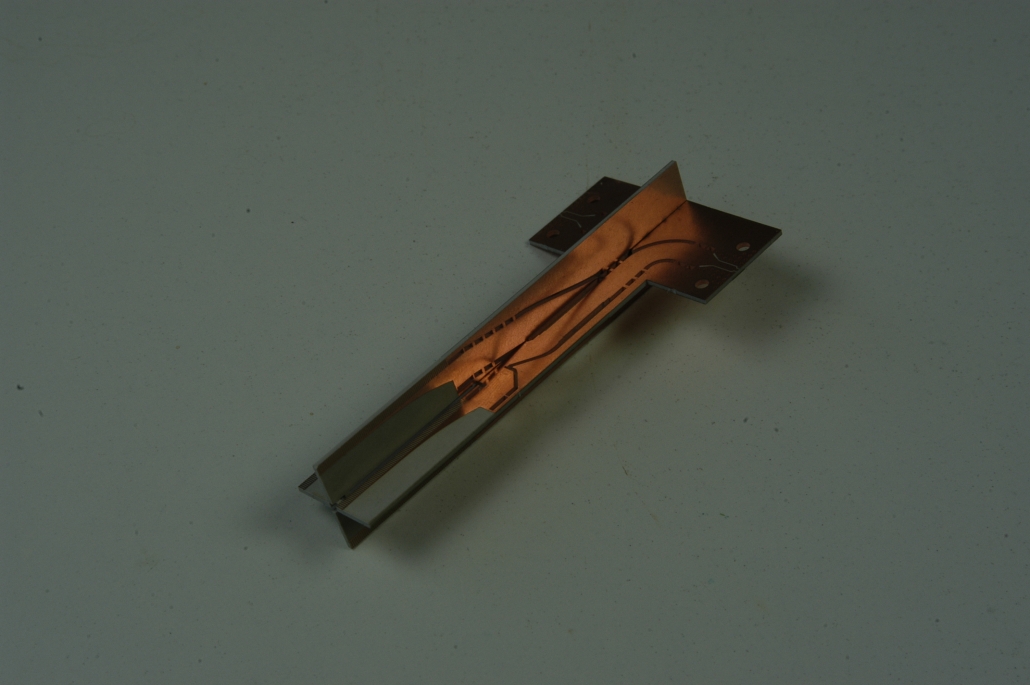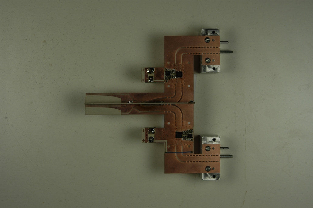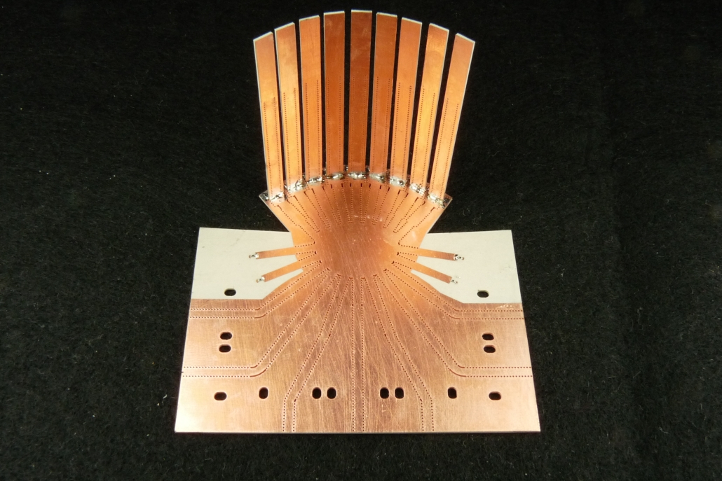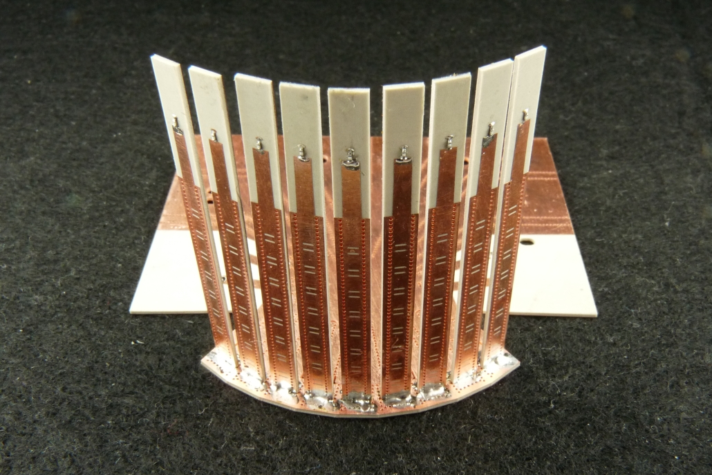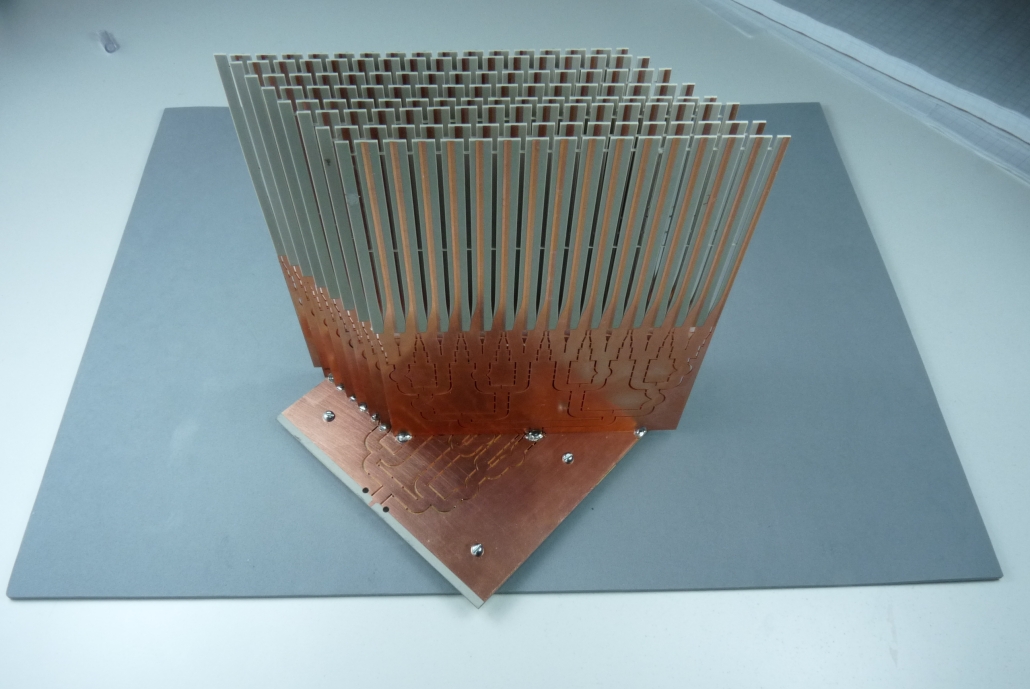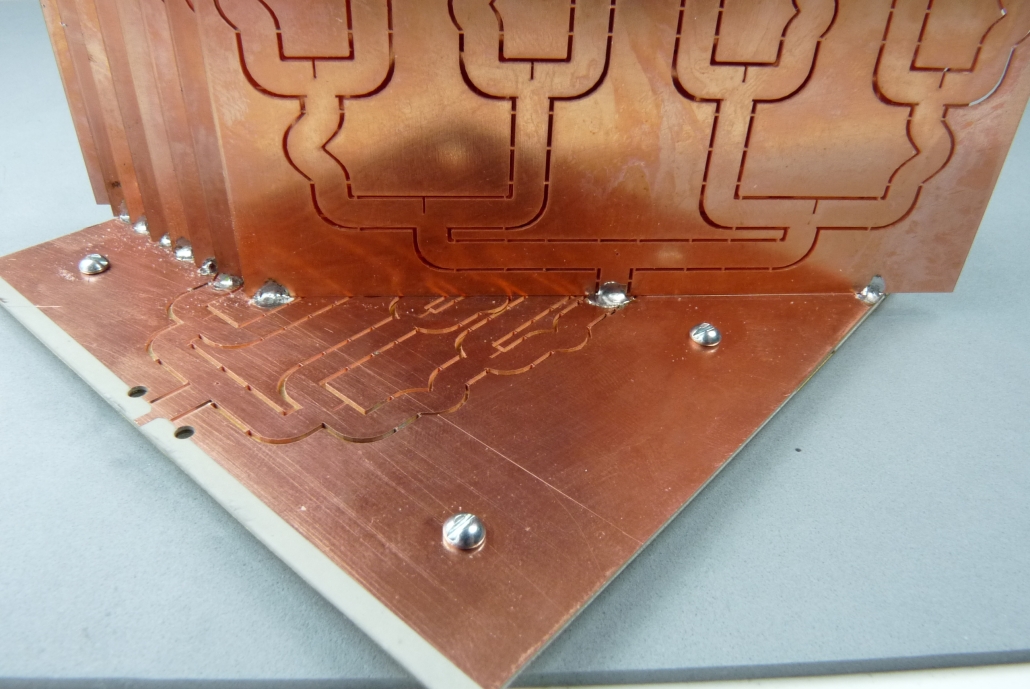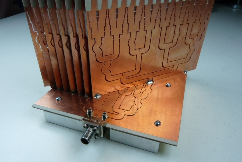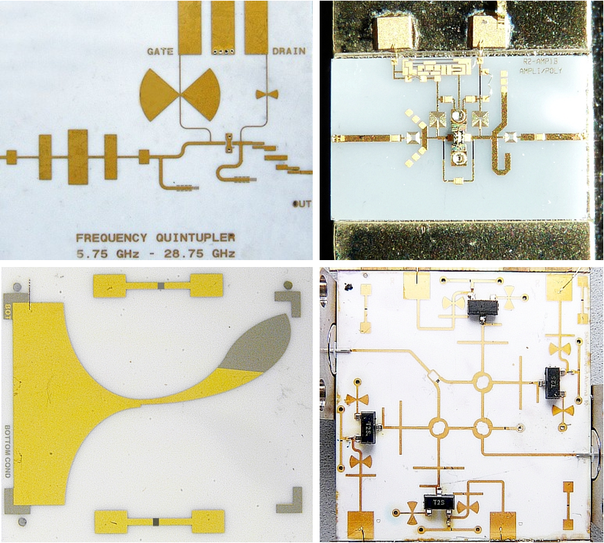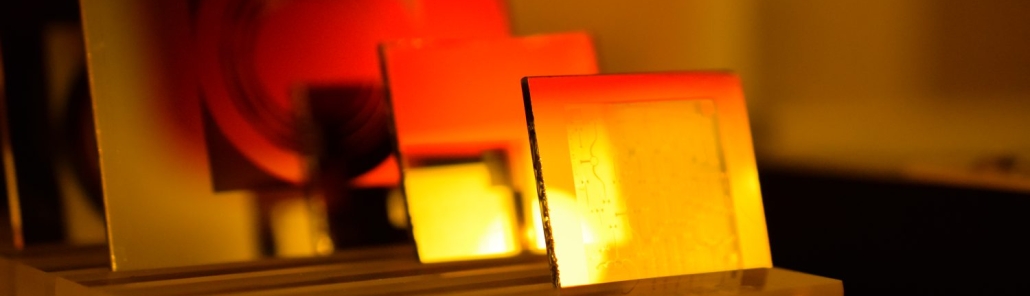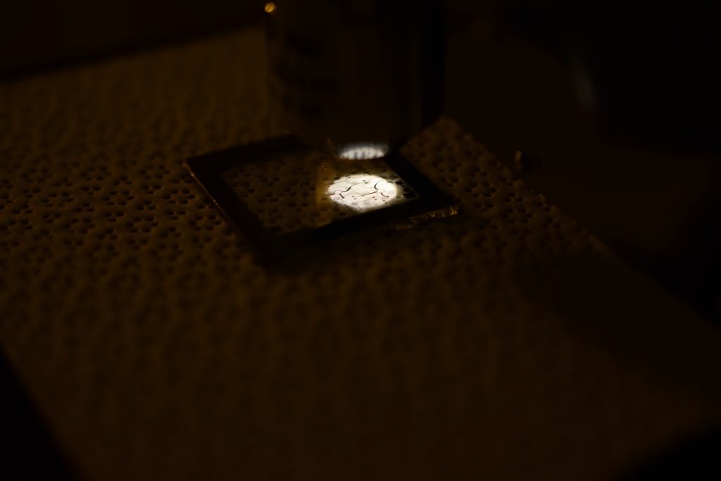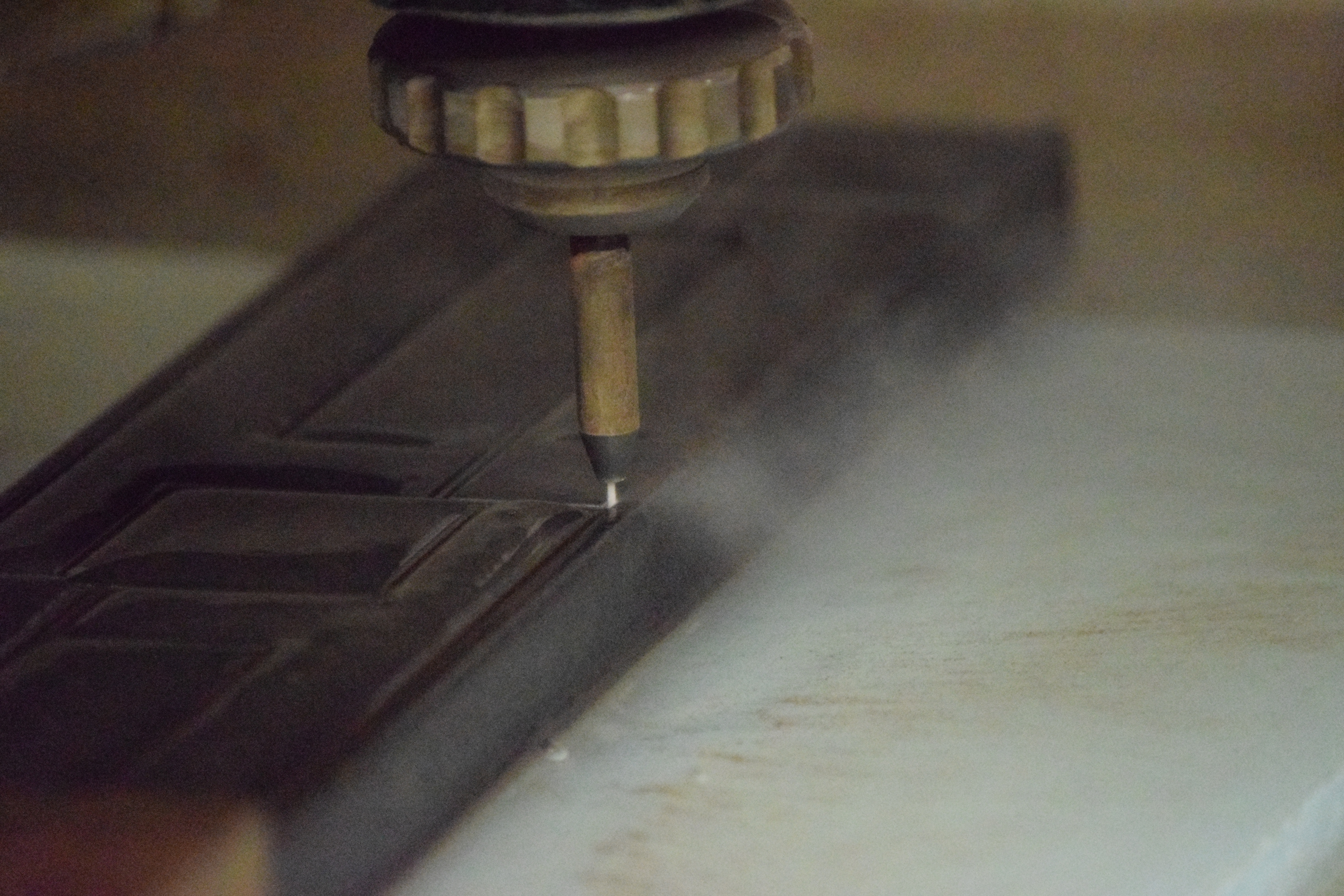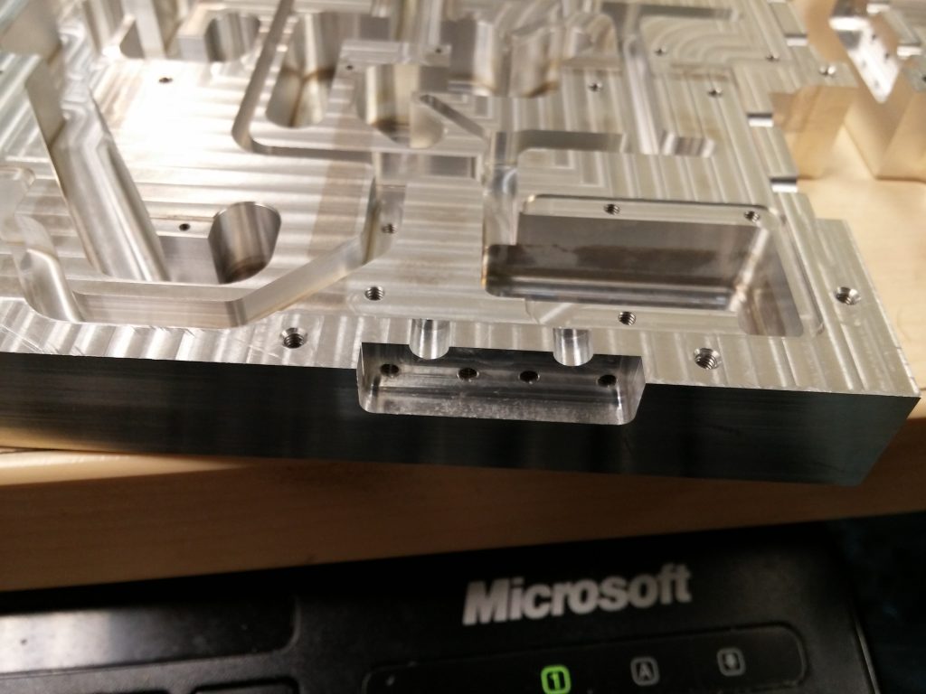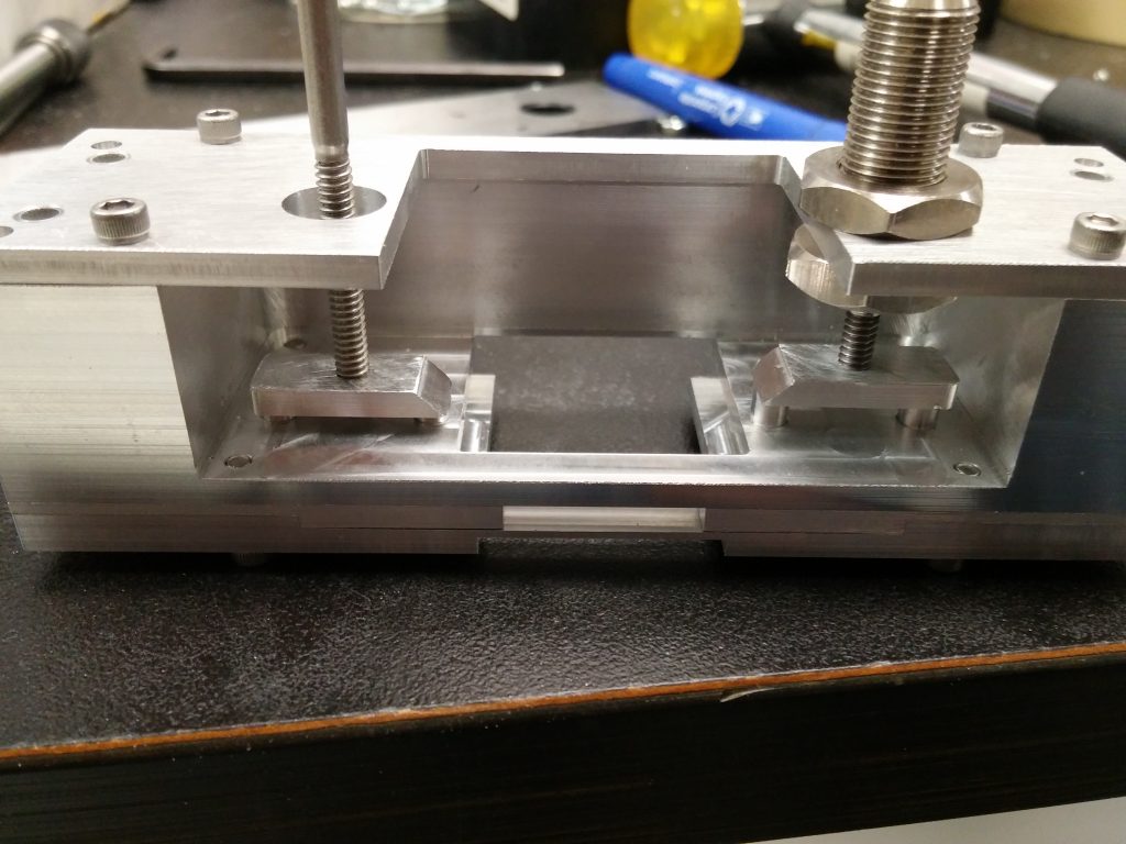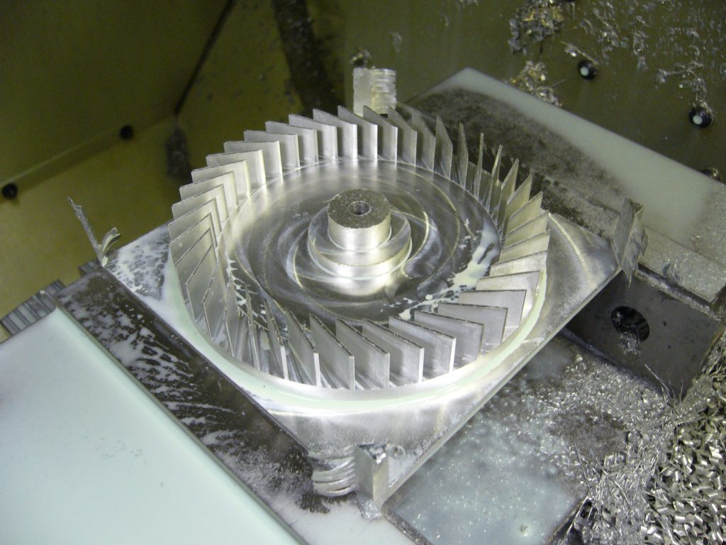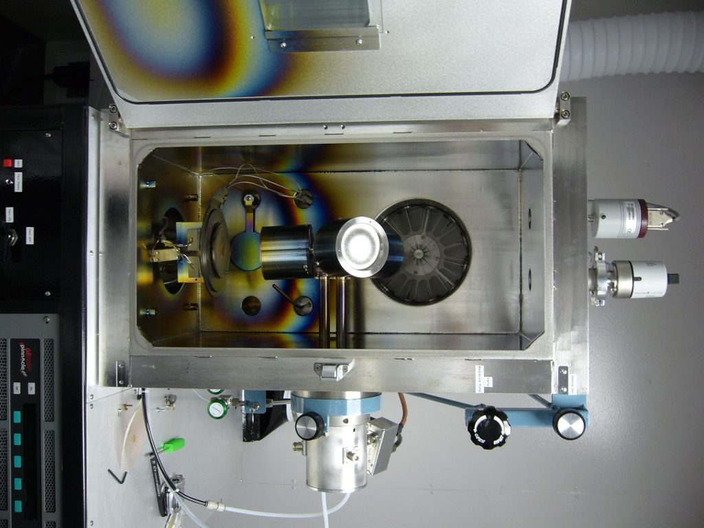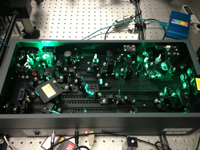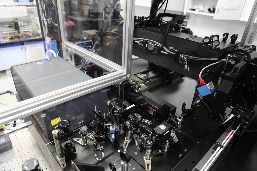
Many technologies for fabrication of microwave circuits are available at Poly-Grames including: printed circuit board on duroid substrates, thin film MHMIC on ceramics, laser machining of metals, ceramics, TMM, etc., and high precision machining on CNC.

MMIC processes are under development. Passive components like capacitors, planar inductors, and air bridges can already be realized.

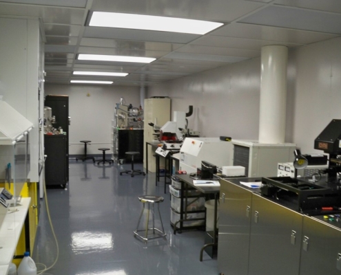
Our fabrication facilities: MHMIC, MMIC, PCB , CNC and assembly line.

IMPORTANT!

Before sending any fabrication file, please take your time and pass the checklist

Please take note, that  if your files don’t comply with the requests, we are not able to process them, hence some major delays will occur.
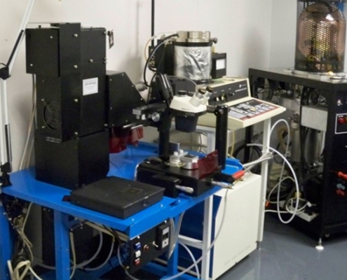
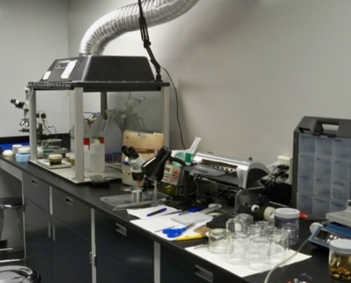
All the tools you need for your PCB fabrication

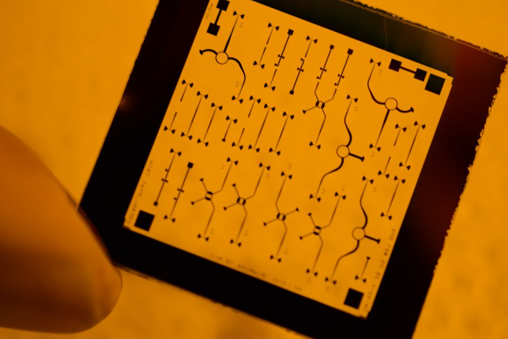
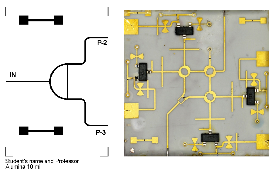
MHMIC Fabrication

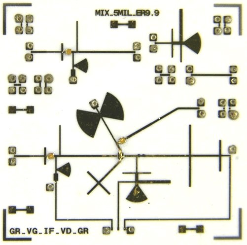
MHMIC Process

Design rules As Fired Substrate

  • Minimum line and Gap  width    = 20 µm
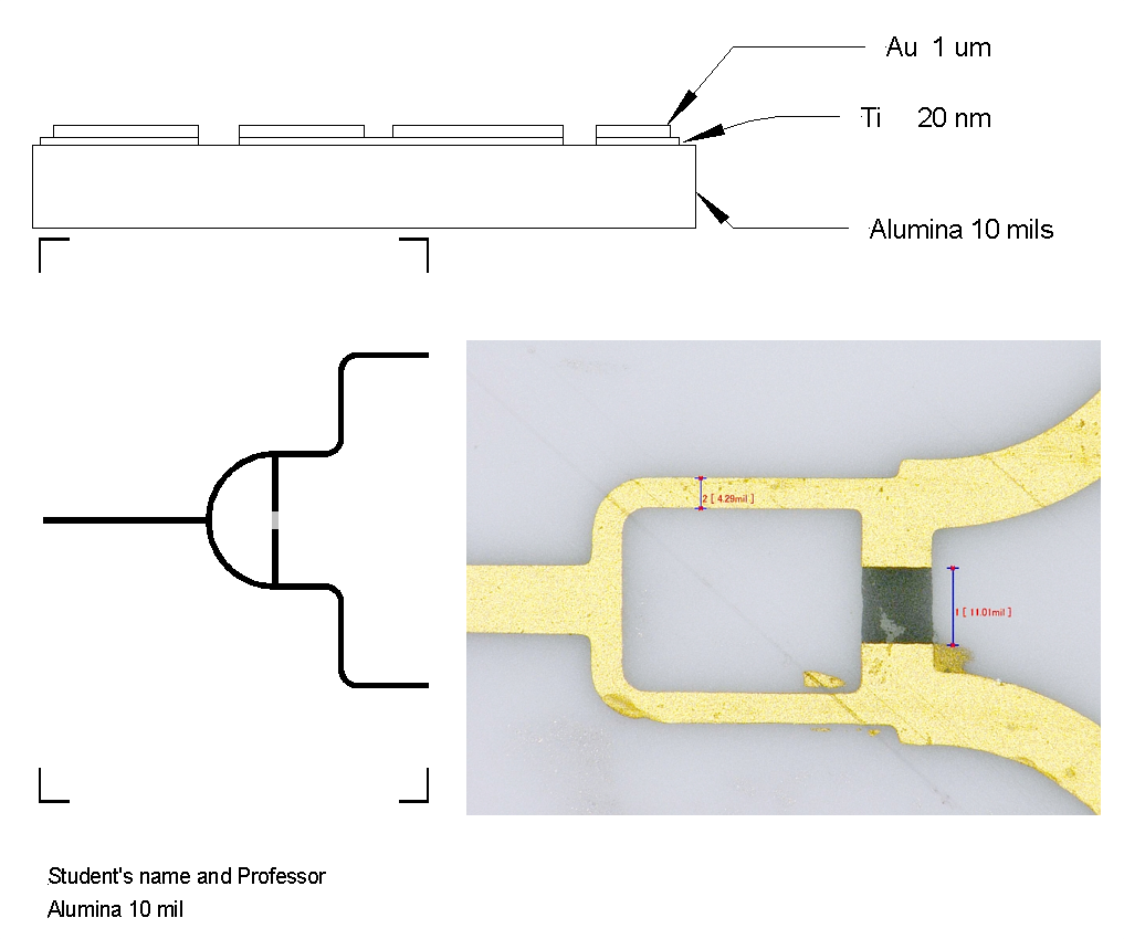
  • Conductor thickness    = 1 µm
  • Conductor material   = Au or Ag
  • Material   = Al2 O3
  • Substrate thickness  =  10 mils
  • Max. size   = up to 1.9 “
  • Er   = 9.9
  • TangΔ  =.001
  • Resistance    = 100 Ώ□
  • Resistor material is Ti   =20 nm thick

MHMIC Lab

Design rules Polish Substrate

  • Minimum line and Gap width   = 10 µm
  • Conductor thickness   = 1 µm
  • Material   = Al2O3 or SiO2
  • Max size   = 1.9″ x 1.9″
  • Substrate thickness  = Up to 30 mils
  • Resistance  = 100 Ώ□
  • Resistor material  is Ti   = 20 nm thick

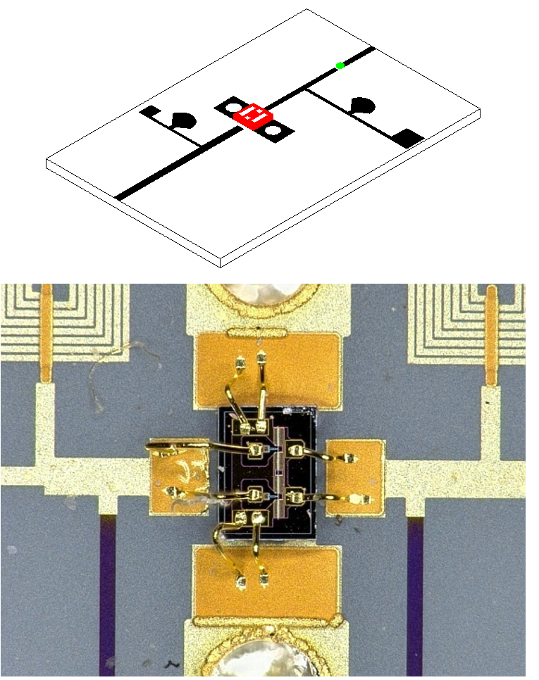
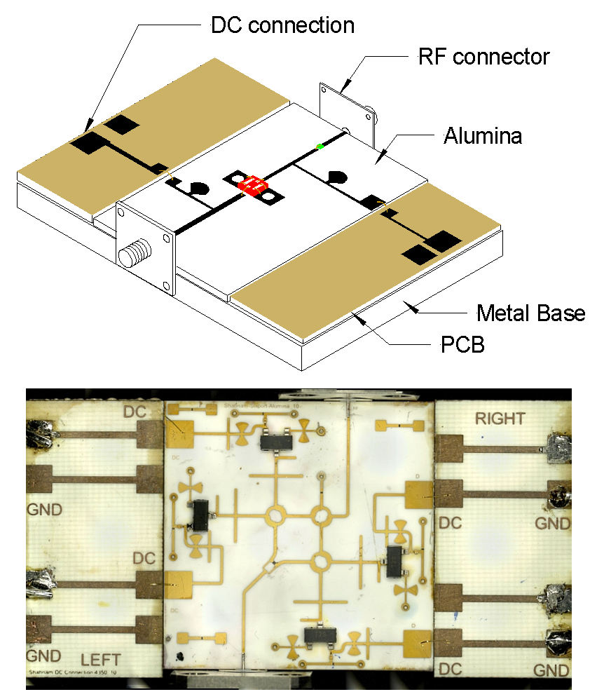
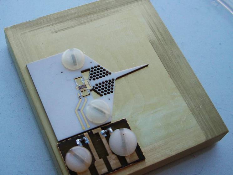
MHMIC Assembly

Practical Advices

  • For RF ground use open with 180° offset rather than hole
  • Take care of connector spacing minimum is 0.5 inch
  • If you planning to use test fixture take care about the offset between connector
  • If you planning  to test with probing station make sure your circuit respect the probe spacing
  • The laser always make hole larger than draw by 1 mil
  • The wire bonding we can provide is 0.7 mil
  • The ribbon is  0.5 X 3 mil
  • Parasitic inductance of wire bonding 20 pH/ mil
  • Minimum pad size for wire bonding  3 mil

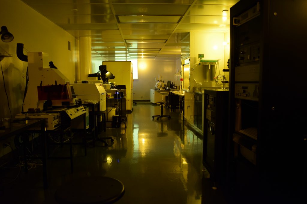
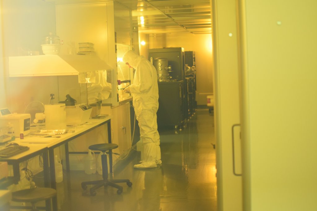
Class 100 Clean Room

Clean Room

Sputtering

Sputtering

Thermal Evaporator

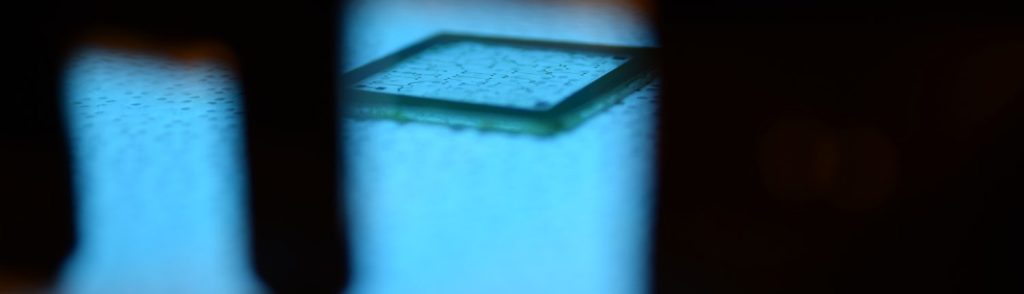
Lithography

Ion Miling

Rapid thermal processing oven

Lithography bench 

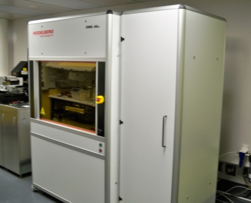
Mask Writer

Minimum feature        1 µm

Max Plate size             200 mm

State of the art machining facilities

CNC & Waterjet Machining

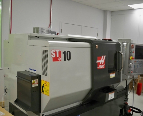
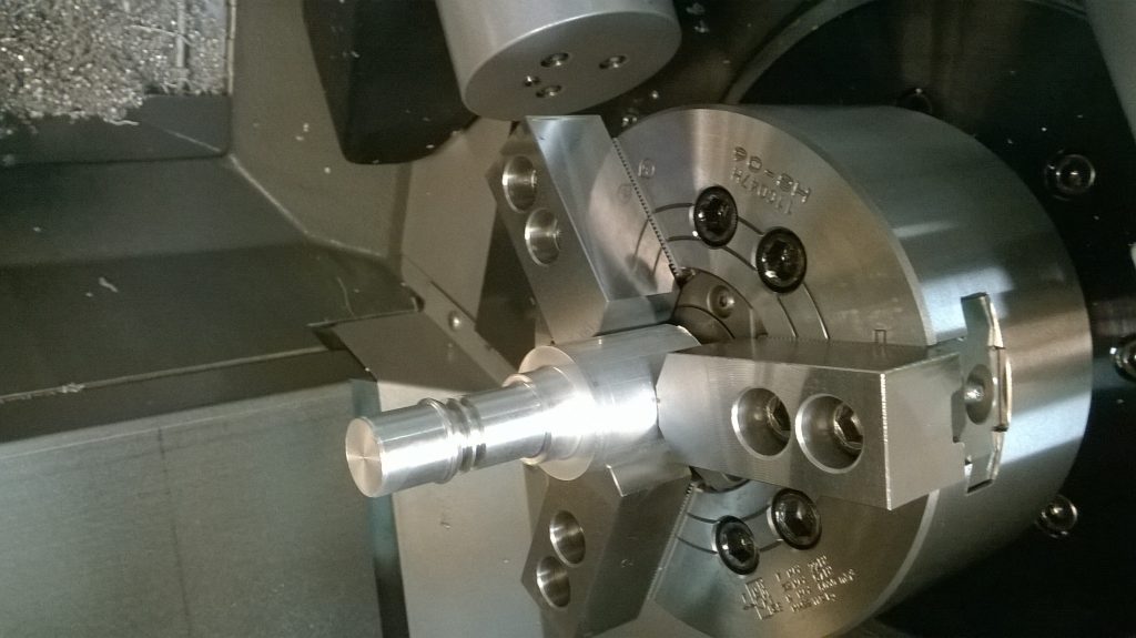
CNC Lathe

Resolution: 12 µm

Max diameter : 300 mm

Max lenght :  300 mm 

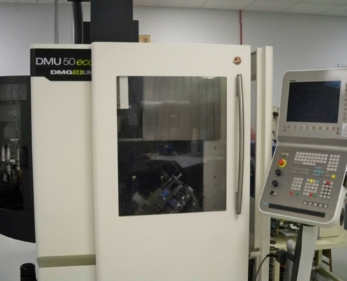
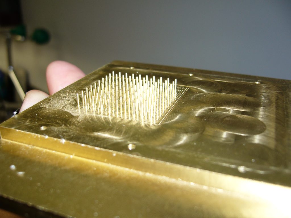
CNC Milling

Resolution (minimum step):  12 µm

Max size X : 500 mm, Y : 450 mm, Z : 400 mm

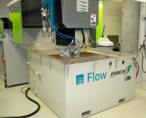
Abrasive Waterjet

Resolution :   25 µm

X-Y disp. :  1.2 m x 1.2 m

Nozzle Dia :  0.8 mm

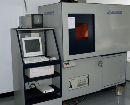
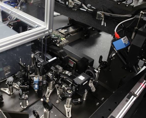
Laser ablation, drilling and cuting are possible at Poly-Grames

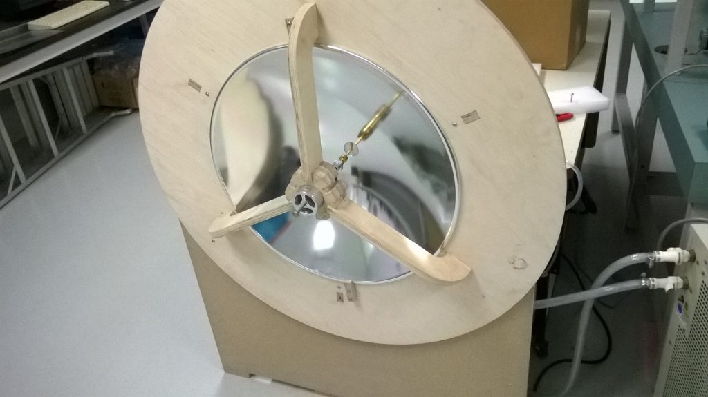
Laser Fabrication

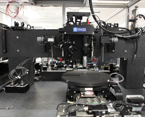
Fabulas 3D micromachining stage

  • Resolution on position : 1 nm
  • Max disp. X-Y: 30 cm x 30 cm 
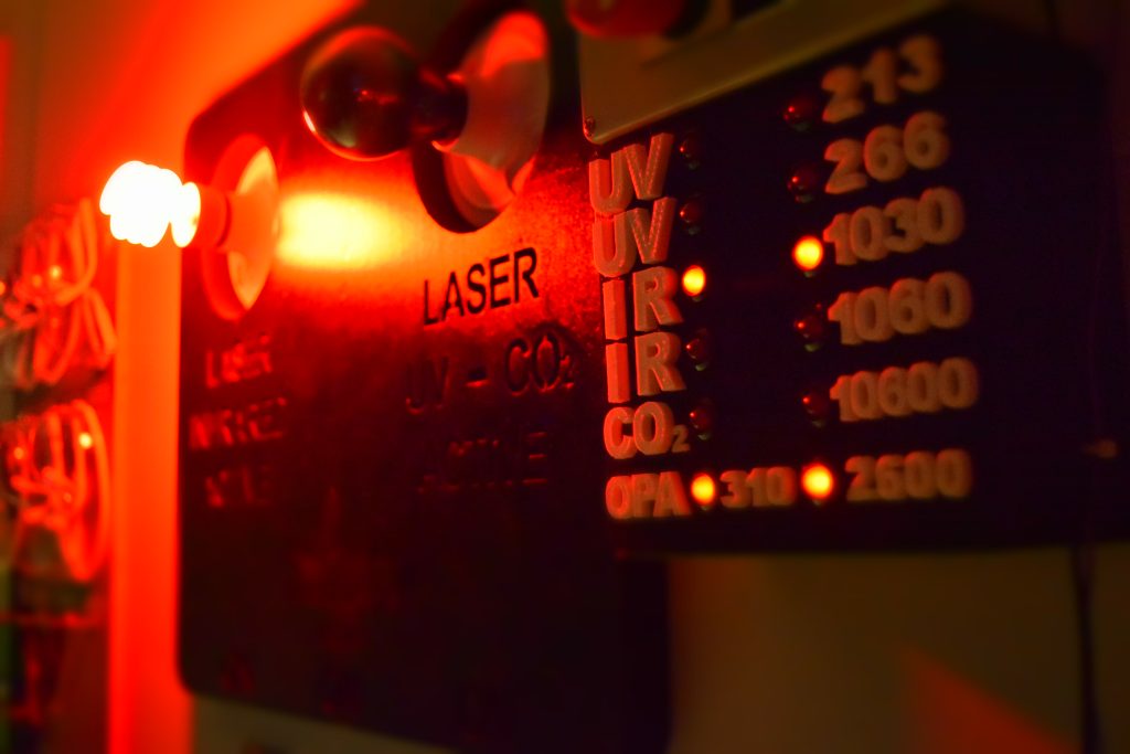
  • Laser wavelengths: 1030 nm, 1060 nm & 10.6 µm 
  • fs laser writing and laser ablation

Laser Micromachining Center

  • Stage displacements (steps) : 2.5 µm
  • X-Y stage : 200 mm
  • NdYag  wavelength : 532 nm
  • Beam Widht : 25 µm

Fabulas 1m FBG writing station

  • Precision on position :   1 nm
  • X disp. :  1.0 m
  • laser wavelengths :  213 nm & 266 nm
  • Tunable Interferometer for writing FBG (0.6µm – 2 µm)
  • FBG by: Talbot Interferometer; Modulators; Phase mask; fs point by point